The BBC Microcomputer has a number of "selectable" links. There are 33 of these links on main printed circuit boards (main PCB's) up to issue 31 subsequent issues having 39 links. It may be that future issues will have more than these 39 links available. This section explains the functions of the various links within the machine.
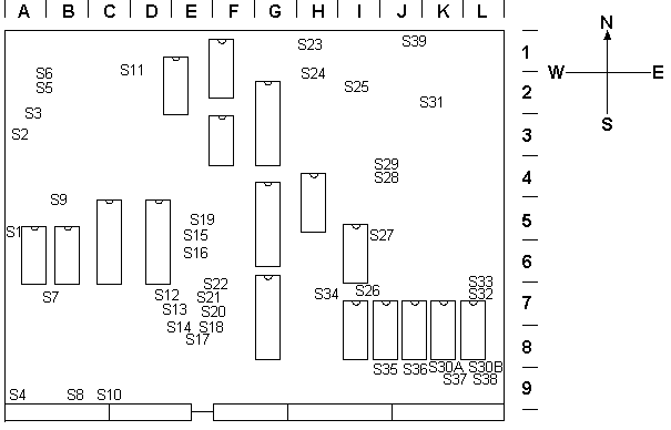
The links are situated at various positions on the main PCB, taking the form of soldered wire, printed track or shorting jumpers. Table 4.1 at the end of this section lists each of the links and provides grid reference information as to their approximate position on the main PCB. This table also identifies the type of link together with the upgrade or expansion with which it deals. Figure 4.1, at the end of this chapter, is a shadow diagram of the main PCB which shows the positions of the various links.
In addition to the links on the main PCB there are 8 more links that can be fitted to the machine, these are situated in the bottom right hand corner of the printed circuit board on which the keyboard is mounted. The keyboard links are shown on the photographs at the end of chapter 5. These keyboard links are not normally fitted on models A or B but some may have to be installed if the floppy disc expansion is to be fitted. For further details see chapter 5.
In order to simplify matters and minimise any ambiguities, the orientation of the various links will be described in terms of the cardinal points of the compass (see shadow diagram fig 4.1).
With the machine placed in front of you in the normal position (with the keyboard facing towards you) the rear of the machine will be referred to as NORTH and the front of the machine as SOUTH. The left and right hand sides will be referred to as WEST and EAST respectively. This is shown diagrammatically in fig 4.1 and on the photographs at the end of chapter 5.
As with all modifications that are to be made to the machine the microcomputer should be completely disconnected from the mains supply before the top cover is removed.
It must be stressed that by making modifications to the links on the main PCB you are likely to invalidate the manufacturers guarantee. If you are in any doubt you should consult your local Acorn dealer.
The top cover can be released by removing the four large fixing screws (which may be marked "FIX") using a No.2 crosspoint screwdriver. The positions of these screws can be seen from the photographs at the end of chapter 5. Two are situated at the rear of the machine and the remaining two are on the underside of the machine beneath the keyboard.
Depending on the particular links that are to be modified it may be necessary to remove the keyboard in order to gain access. Links S4, 58, S10, S14, S17, S18, and S30 are those in question on boards up to issue 3. Boards from issue 4 onwards also have links S35, S36, S37 and S38 beneath the keyboard.
At this stage one must consider the particular links that are to be modified. Table 4.1 at the end of this section specifies whether a particular link is soldered wire, copper track or a jumper.
If any of the soldered wire links are to be modified then the main PCB may have to be removed from the base to allow access to the underside of the PCB.
The keyboard assembly can be detached by removing the two nuts and bolts situated on either side of the keyboard PCB (please note that some main PCB's prior to issue 4 have two keyboard securing bolts on the left hand side of the keyboard PCB) . The location of these bolts can be seen from the photographs in chapter 5. The next step in removing the keyboard assembly is to carefully unplug the interconnecting ribbon cable from the main PCB (PL13) and also the loudspeaker connector from PL15.
The keyboard can now be safely set aside to reveal the main PCB beneath.
Before the main PCB can be removed the two wires from the BNC "video out" socket on the rear of the case must be disconnected. On early issue boards these two wires were soldered but some later issues use push fit connectors. It is important to note which of the two wires is the signal wire and which is the ground wire, so that they can be replaced correctly. It is suggested that the ground wire be marked by placing a piece of coloured insulating sleeving over the wire. On some late issue boards black (0V) and red (signal) wires are fitted as standard.
The next step is to remove each of the seven power supply cables from the main PCB. It is important to take care when removing these cables as a reasonable amount of force may be required. It is particularly important not to bend the flat PCB pins backwards and forwards because they can easily fracture.
All that remains now, is to remove the four screws which secure the main PCB to the base with a No.2 crosspoint screwdriver. The positions of these screws are shown in the photographs at the end of chapter 5. The PCB can now be removed from the base and carefully placed on a work surface which should be clean and free from static charge. The ideal working surface would be an electrically conductive sheet (perhaps aluminium foil) connected via a 1 Megohm resistor to earth. Chapter 2, gives more details on static precautions and working environment. As some of the following description involves handling of MOS devices it is strongly recommended that the reader should be familiar with the section on static hazards as detailed in that chapter.
Before describing the function of each individual link on the main PCB, the procedure for re-assembling the microcomputer will be described.
Re assembly is essentially the reverse of the dismantling procedure with the main PCB being replaced before the keyboard PCB. There are, however, a number of points to note
| Link No. | Position. | Function. | ||||||||||||||||||||
| 1 | Printer strobe select; Only present on issue 4 boards onwards. Selects the type of printer strobe output to pin 1 of PL9 (printer port); |
|||||||||||||||||||||
| SOUTH | Printer strobe output taken directly from CA2 output
of IC69 (VIA) i.e. Centronics standard. |
|||||||||||||||||||||
| NORTH | Printer strobe output with "current sink" capability. | |||||||||||||||||||||
| 2 | Econet Non Maskable Interrupt (NMI). This link must not be fitted with IC91 (74LS132) in place. Note this link must fitted in order for the floppy disk interface to be able to produce a NMI; |
|||||||||||||||||||||
| FITTED | Disables the Econet NMI function. | |||||||||||||||||||||
| REMOVED | Enables the Econet NMI function. | |||||||||||||||||||||
| 3 | Econet clock base frequency selection. Only used on issues prior to 4, consult circuit diagram and "Econet" manual. If the microcomputer is to be used as the network clock source then the clock frequency is set using this group of 9 links together with link S6. The frequency can be set in the range 75 to 625 kHz. In practice the frequency setting will depend upon the length of the network. See chapter 3 for a more detailed explanation. Link S3 actually sets the base clock frequency which can then be further subdivided by either 4 or 2 using link S6. If a jumper is installed in a particular position on S3 then that base clock frequency is selected. The circuit given in figure 5.4 shows this more clearly.
|
|||||||||||||||||||||
| 4 | Floppy disc size selection | |||||||||||||||||||||
| EAST | Selected when a 5 1/4 inch floppy disc drive is to be
used. Connects pin 32 of PL8 to side select on floppy disc drive. |
|||||||||||||||||||||
| WEST | Selected when an 8 inch floppy disc drive is to be
used. Connects pin 2 of PL8 to side select on floppy disc drive. |
|||||||||||||||||||||
| 5 | Econet clock; Only used on issues prior to 4 See description for link S3. |
|||||||||||||||||||||
| NORTH | Enable Econet clock. | |||||||||||||||||||||
| SOUTH | Disable Econet clock. | |||||||||||||||||||||
| 6 | Econet clock division; Only used on issues prior to 4. See also links 53 and 55. |
|||||||||||||||||||||
| NORTH | Divide Econet base clock frequency by 2 | |||||||||||||||||||||
| SOUTH | Divide Econet base clock frequency by 4 | |||||||||||||||||||||
| 7 | Count/OPI Sets the logic level on pin 30 of IC78 (P8271) the floppy disc controller. This link enables or disables this function by applying 0 volts or 5 volts to pin 30. The function is normally enabled. Consult the Manufacturers data sheet at the end of the manual for further information. |
|||||||||||||||||||||
| WEST | Applies 5 volts to pin 30 of IC78. | |||||||||||||||||||||
| EAST | Applies 0 volts to pin 30 of IC78 thus enabling Count/OPI. This is the normal position. | |||||||||||||||||||||
| 8 | Disc head load function; This link is used to connect the read/write head load line to pin 16 on PL8 ("disc drive" connector). |
|||||||||||||||||||||
| INSERTED | Connects read/write head load signal to PL8. Normally inserted when floppy expansion is installed. | |||||||||||||||||||||
| REMOVED | Disconnects to read/write head load signal to PL8. | |||||||||||||||||||||
| 9 | Floppy disc NMI selection This link must not be inserted with IC70 (P8271) in place. There is a serious PCB fault associated with link S9 on boards prior to issue 4. On issues 1 and 2 pins 9 & 7 of IC27 must be linked in order to enable the floppy disc NMI. Some late issue B boards have link S9 as a PCB track which must be cut to enable floppy disc NMI. Chapter 5 (machine upgrading) gives more detailed information on this link. Chapter 6 (Hints Tips and modifications) covers the modifications in more detail. |
|||||||||||||||||||||
| INSERTED | Disable floppy disc NMI. | |||||||||||||||||||||
| REMOVED | Enables floppy disc NMI. | |||||||||||||||||||||
| 10 | Floppy disc size selection; Connects index input from floppy disc controller (IC78) to either pin 8 (5 1/4 inch) or pin 4 (8 inch) of PL8. |
|||||||||||||||||||||
| WEST | Selects 5 1/4 inch size floppy disc. | |||||||||||||||||||||
| EAST | Selects 8 inch size floppy disc. | |||||||||||||||||||||
| 11 | Econet station address; The "Econet" local area network system can support a maximum of 254 stations plus one "file server" and one "print server". Each of these 254 stations can have a unique address which is set by link S11. Link S11 is in fact a group of eight links each one corresponding to one of the eight binary address digits thus it is possible to select a unique address in the range C to 255. The links go from NORTH to SOUTH least significant to most significant respectively. |
|||||||||||||||||||||
| INSERTED | Logic 0. | |||||||||||||||||||||
| REMOVED | Logic 1. | |||||||||||||||||||||
| 12 | Paged ROM select line A (LSB) This link along with link S13 is used to enable/disable paged ROM selection. Note that the paged ROM selection facility can only be used with operating Systems 1.0 or greater. Do not fit IC76 (74LS163) with this link inserted. |
|||||||||||||||||||||
| INSERTED | ROM select line pulled down to 0V; i.e. disable LSB
of paged ROM selection. Normal position for model A machines. |
|||||||||||||||||||||
| REMOVED | ROM select line taken from output A of IC76. i.e.
enable LSB of paged ROM selection. Normal position on model B machines which were fitted with operating systems from version 1.0 onwards. |
|||||||||||||||||||||
| 13 | Paged ROM select line B. (bit 2 in 1 2 4 8 binary system) Do not fit IC76 (74LS1633) with this link inserted. See description for link S12 above. |
|||||||||||||||||||||
| INSERTED | ROM select line B connected to 0V; i.e. disable bit 2 of paged ROM selection. Normal position for model A machines. |
|||||||||||||||||||||
| REMOVED | ROM select line taken from output B IC76. i.e. enable bit 2 of paged ROM selection. Normal position on model B machines. |
|||||||||||||||||||||
| 14 | JIM (NPGFD) enable/disable. The memory map of the machine is organised to allow devices connected to the 1 MHz bus to be able to freely access machine addresses in the range &FD00 to &FDFF (JIM) and &FC00 to &FCFF (FRED). In order to provide this function the machine operating system ROM, which would normally map into this space, must be disabled. The links S14 and S17 allow this to be done by disabling the outputs of all RAMs when the address bus holds an address in this range. See also link s17. If S14 is REMOVED then S16 must be INSERTED. |
|||||||||||||||||||||
| INSERTED | Disables all ROM outputs when the address bus holds
an address in the range JIM (&FD00 to &FDFF). This is the normal position. |
|||||||||||||||||||||
| REMOVED | Enables ROM outputs when the address bus holds an
address in the range JIM (&FD00 to &FDFF) |
|||||||||||||||||||||
| 15 | JIM (NPGFD) fast access. This link uses IC23 (74LS30) to enable/disable fast access to addresses in the range &FD00 to &FDFF (JIM). IC23 (74LS30) is used to control the "cycle stretch" function in order to produce the 1 MHz 6502 bus cycle which is required by the 1 MHz bus, the ADC and the system and user VIAs etc. See circuit description in chapter 3. Link S15 must be INSERTED if link S17 is REMOVED; |
|||||||||||||||||||||
| INSERTED | Disables fast access to JIM (&FD00 to &FDFF) i.e. normal position allowing 1 MHz bus to be used normally. | |||||||||||||||||||||
| REMOVED | Enables fast access to JIM (&FD00 to &FDFF) i.e. does not allow the 1MHZ bus to be used normally. | |||||||||||||||||||||
| 16 | FRED (NPCFC) fast access. This link uses IC23 (74LS30) to enable/disable fast access to addresses in the range &FC00 to &FCFF (FRED). See description for link S15. Link S16 must be INSERTED if link S14 is REMOVED |
|||||||||||||||||||||
| INSERTED | Disables fast access to FRED (&FC00 to &FCFF) i.e. normal position allowing the 1 MHz bus to be used normally. | |||||||||||||||||||||
| REMOVED | Enables fast access to FRED (&FC00 to &FCFF) i.e. does not allow the 1 MHz bus to be used normally. | |||||||||||||||||||||
| 17 | FRED (NPGFC) enable/disable. See the description for link S14. If S17 is REMOVED then S15 must be INSERTED |
|||||||||||||||||||||
| INSERTED | Disables all ROM outputs when the address bus holds an address in the range FRED (&FC00 to &FCFF). This is the normal position. | |||||||||||||||||||||
| REMOVED | Enables ROM outputs when the address bus holds an address in the range FRED (&FC00 to &FCFF) | |||||||||||||||||||||
| 18 | IC100 ROM access speed selection. IC100 is one of the two auxiliary ROMs. The machine offers the facility to use slow access speed devices in this position. In slow access mode the chip select signal for IC100 is at 1 MHz derived via IC23 (74LS30) . This facility was used in early issue machines where the operating system was fitted into four 2732 type EPROMs because the 2732 used were slow access speed types. |
|||||||||||||||||||||
| SOUTH | IC100 chip select run at 1MHZ. Slow access. | |||||||||||||||||||||
| NORTH | IC100 chip select run a t 2MHZ. Fast access. | |||||||||||||||||||||
| 19 | IC52, IC88 and IC101 ROM access speed selection. The machine has three diodes installed on the main PCB that are used to alter the access speeds for the ROM's IC52, IC88 and IC101. These diodes are D12, D11 and D10 respectively. If link S19 is in the WEST position then the chip select lines of these three ROMs are connected via the diodes to the slow access control NAND gate (IC23 -74LS30) Thus these ROMs are accessed at slow speed when the diodes are installed and link S19 is in the WEST position. The diodes can be individually removed thus allowing any one or more of the ROMs to be accessed at fast or slow speed. |
|||||||||||||||||||||
| WEST | If the relevant diode is installed then its associated ROM is accessed at slow speed. If the diode is removed then the associated ROM is accessed at full speed. | |||||||||||||||||||||
| EAST | All three ROM's are accessed at full speed. The diodes have no effect. | |||||||||||||||||||||
| 20 | ROM selection decoding. IC20 (74LS139) is a dual 2 to 4 line decoder. Half of this device is used to select the 4 sideways ROM sockets occupied by IC52, IC55, IC100 and IC101. The two line input to this decoder can be taken from either the two LSB outputs of IC70 (74LS163) or from address lines A12 and A13. The 4 bit code present on the output lines of IC76 is taken from the four least significant data bus lines (D0-D3) and loaded by the high to low transition of the machines ROM select (ROMSEL) signal When this 4 bit code has been loaded in to IC76, the outputs are clocked by IC30 (74LS74) Link S20 selects the input source for the most significant of the two input lines for IC20. Similarly, link S22 is used to select the input source for the least significant of the two input lines for IC20. |
|||||||||||||||||||||
| SOUTH | MSB input of IC20 taken from address line A13. | |||||||||||||||||||||
| NORTH | LSB input of IC20 taken from ROMSEL line via IC76 (74LS163) | |||||||||||||||||||||
| 21 | ROM memory mapping selection. Note that link S21 is a dual link i.e. 2 x NORTH/SOUTH or 2 x EAST/WEST. The machine offers the facility to alter the ROM memory map The machine offers the facility to alter the ROM memory map in two consecutive 16K byte ranges. These two ranges lie at the top of the machine's address map From 32k to 64k (&8000 to &FFFF) i.e. the ROM socket for IC51, which normally contains the operating system ROM, can be mapped into either of two address ranges. The normal 16k byte range is &C000 to &FFFF but link S21 allows this to he changed to &8000 to &BFFF. Whichever 16K byte range is selected for IC51 the sideways ROM sockets (IC52, IC100 and IC101) will map into the remaining 16K byte range. Thus, in a normally configured machine, if the operating system ROM IC51 occupies addresses &C000 to &FFFF then the sideways ROMs will occupy addresses in the range &8000 to &BFFF. Conversely if the operating system ROM were to be mapped into addresses in the range &8000 to &BFFF then the sideways ROMs would be mapped into addresses in the range &C000 to &FFFF |
|||||||||||||||||||||
| 2 x NORTH/ SOUTH |
IC51 mapped into address range &8000 to
&BFFF. sideways ROMs mapped into address range &C000 to &FFFF. |
|||||||||||||||||||||
| 2 x EAST/ WEST |
IC51 mapped into address range &C000 to
&FFFF. Normal configuration. Sideways ROM's mapped into address range &8000 to &BFFF; Normal configuration. |
|||||||||||||||||||||
| 22 | ROMSEL (romselect) line use. The sideways ROM selection mechanism is covered in the functional description or link S20. | |||||||||||||||||||||
| SOUTH | LSB input of IC20 (74LS139) taken from address line A12. | |||||||||||||||||||||
| NORTH | LSB input of IC20 taken from ROMSEL line via IC76 (74LS163) | |||||||||||||||||||||
| 23 | RS423 Received data line termination. A facility is provided on IC74 (DS88LS120N) to enable the received data line (DATA IN) and the clear to send line (CTS) to be terminated This is not necessary at moderate baud rates or when relatively short data leads are used. It may, however, be necessary at high baud rates or with long data leads. For more details consult the manufacturer's data sheet which is included at the end of this book. See also link S24. |
|||||||||||||||||||||
| INSERTED | Receiver terminated | |||||||||||||||||||||
| REMOVED | Receiver not terminated. Normal position. | |||||||||||||||||||||
| 24 | CTS (clear To Send) line termination. See description for link S23. | |||||||||||||||||||||
| INSERTED | CTS line terminated. | |||||||||||||||||||||
| REMOVED | CTS line not terminated. This is the normal position. | |||||||||||||||||||||
| 25 | Column Address Selection (CAS) The machine's dynamic RAM memory is effectively organised into two columns each of 16K bytes. The first 16K column occupies addresses &0000 to &3FFF and is selected by the CAS1 line (i.e. as in the model A machine). The second column occupies addresses in the range &4000 to &7FFF and is selected by CAS0 as in the model B machine. This link is used to enable CAS0 to function thus enabling a total of 32k bytes of RAM memory to be addressed. |
|||||||||||||||||||||
| SOUTH | CAS0 disabled thus only 16K bytes (&0000 to
&03FF) can be addressed. This is the normal position for the model A machine. |
|||||||||||||||||||||
| NORTH | CAS0 enabled thus allowing RAM memory in the range &4000 to &7FFF to be addressed. This is the normal position for the model B machine. | |||||||||||||||||||||
| 26 | Inverse video selection. The machine has the facility to provide either inverted or non inverted (normal) video outputs. This applies to both the composite video output (the "video out" socket at the rear of the machine) the UHF modulated output and the primary colour output (RGB). Normal composite video will give light characters on a dark background whilst inverted composite video will give dark characters on a light background; |
|||||||||||||||||||||
| WEST | Normal video output. | |||||||||||||||||||||
| EAST | Inverted video output. | |||||||||||||||||||||
| 27 | Floppy disc clock speed selection. | |||||||||||||||||||||
| WEST | Selects an 8 MHz base clock frequency. For use with 5 1/4 inch floppy disc drives. |
|||||||||||||||||||||
| EAST | Selects a 16 MHz base clock frequency For use with 8 inch floppy disc drives. |
|||||||||||||||||||||
| 28 | Cassette interface baud-rate selection. It is possible to alter the baud rate of the cassette interface using links S28 and S29. Note that if link S28 is in the EAST position then the RS423 baud rate is also affected. |
|||||||||||||||||||||
| WEST | Selects the base baud rate from the baud rate generator IC42 (74LS163) i.e. the normal 1200 baud position. | |||||||||||||||||||||
| EAST | Selects 1300 baud for cassette interface. | |||||||||||||||||||||
| 29 | Cassette interface baud rate selection. See the description of link S28. Note that with S29 in the WEST position the RS423 baud rate will also be affected; |
|||||||||||||||||||||
| EAST | Selects the base baud rate from the baud rate generator IC42 (74LS163) i.e. the normal 1200 baud position. | |||||||||||||||||||||
| WEST | Selects 1300 baud for cassette interface. | |||||||||||||||||||||
| 30 | ||||||||||||||||||||||
| 31 | RGB synchronisation (CSYNC) polarity. The CSYNC signal which is used to synchronise the line time base can be selected as positive or negative going. Some video monitors may require the CSYNC signal to be inverted in order to work correctly; |
|||||||||||||||||||||
| WEST | Positive going CSYNC signal. Normal position. | |||||||||||||||||||||
| EAST | Negative going CSYNC signal. | |||||||||||||||||||||
| 32 | ROM type selection for IC52 & IC88. Links S32 and S33 allow different types and sizes of ROMs to be used in place of IC52, IC88 and IC100, IC101 respectively. |
|||||||||||||||||||||
| WEST | Address bus line A13 is connected to A13 of IC52 & IC88. This is the normal selection for using 16K ROMs. | |||||||||||||||||||||
| EAST | Plus 5 volts is connected to A13 of IC52 & IC88. | |||||||||||||||||||||
| 33 | ROM type selection for IC100 &IC101 See description for link S32. |
|||||||||||||||||||||
| WEST | Address bus line A13 is connected to A13 of IC100 & IC101. This is the normal selection for using 16K ROMs. | |||||||||||||||||||||
| EAST | Plus 5 volts is connected to A13 of IC100 & IC101. | |||||||||||||||||||||
| 34 to 38 |
Sideways ROM chip select signals. These links are only present on main circuit boards from Issue 4 onwards. They are used to select the source for the chip select signals that are used to select the machine's internal ROM's. The links apply to ROM's IC5l, IC52, IC88, IC100 and IC101 respectively the Acorn circuit diagram shows this more clearly. Note these links are normally inserted. |
|||||||||||||||||||||
| 39 | Composite video colour selection. This link is only present on boards from issue 4 onwards. It gives the user the option of having a monochrome or colour output signal from the "video out" socket at the rear of the machine. Chapter 6 details a modification that can be installed on any issue board to allow the video out socket to provide a colour output. Note: It is not advisable to insert this link when usinq a monochrome monitor, as this may cause "ghosting" |
|||||||||||||||||||||
| REMOVED | Monochrome video output. | |||||||||||||||||||||
| INSERTED | Colour video output (PAL). |
As mentioned above there is a facility provided on the BBC Microcomputer's keyboard PCB to allow jumpers to be installed, the position of the holes that are there to take these jumpers can be seen in the photographs at the end of chapter 5.
At the present time when the machines are manufactured there are no links fitted across these holes on either the model A or B machine.
A machine which was purchased with the floppy-disc upgrade already fitted may, however, have certain of the links inserted. This will depend upon the type of floppy disc drives that were sold with the microcomputer.
The keyboard links are extremely useful and the functions that they control are likely to be ones that the average user would want to change fairly frequently. For this reason it is not a good idea to use soldered wire links, as these are difficult to alter. Indeed if the links were unsoldered and resoldered a number of times the PCB would eventually become damaged.
The ideal solution to this problem is to use an eight-way dual in-line switch (DIL) such as the one shown in the photograph at the end of chapter 5.
These switches are available from a number of electronic hobbyist sources or from RS Components part no. 337-560. They should fit readily into the holes provided without any modifications. On some keyboard PCB's the copper track is not roller tinned and this may cause slight difficulty when soldering.
As with all modifications to the microcomputer that involve dismantling the machine and soldering, take great care and read chapter 2 before starting any work.
The link functions themselves are detailed in tables 4.3 to 4.6 shown below. Note that the links are numbered from WEST to EAST 1 to 8 respectively.
Table 4.3 - Link functions
| Link Nos. | Link function |
| 1 | 40/80 Track select |
| 2 | Acorn extended mode. |
| 3 & 4 | Floppy disc drive type: i.e. allows drives with a range of access times to be used. See Table 4.4 |
| 5 | Auto boot selection. see table 4.5. |
| 6 & 7 & 8 | Screen mode at power up or break. See table 4.6. |
Table 4.4 - Floppy disc drive type selection
| Link settings. | Action | |
| 3 | 4 | |
| Unmade | unmade | For use with Olivetti, Tandy and Cumana (Teac) drives. |
| Unmade | Made | for use with MPI or similar drives. |
| Made | Unmade | For use with Tandon and Shugart drives with 6 msec access times. |
| Made | Made | Tandon with 4 msec access time. |
TABLE 4.1
| Link No. | Grid | Type | Expansion/Upgrade |
| 1 | A,5 | W | Printer |
| 2 | A,3 | W | Econet |
| 3 | A,2 | J | Econet |
| 4 | A,9 | T | Floppy Disc. |
| 5 | A,2 | J | Econet |
| 6 | A,2 | J | Econet |
| 7 | B,7 | T | Floppy Disc. |
| 8 | B,9 | T | Floppy Disc. |
| 9 | B,4 | W | Floppy Disc. |
| 10 | C,9 | T | Floppy Disc. |
| 11 | C,2 | J | Econet |
| 12 | E,7 | W | ROMs |
| 13 | E,7 | W | ROMs |
| 14 | E,8 | T | ROMs |
| 15 | E,5 | T | NPCFD (JIM) |
| 16 | E,6 | T | NPCFC (FRED) |
| 17 | E,8 | T | MPCFC (FRED) |
| 18 | E,8 | J | IC100 ROM. |
| 19 | E,5 | J | IC52, 88, 101 ROMs |
| 20 | E,7 | J | ROMs |
| 21 | E,7 | J | IC51 |
| 22 | F,7 | J | ROMs |
| 23 | H,1 | T | RS423 |
| 24 | H,2 | T | RS423 |
| 25 | I,2 | J | RAM (16K/32K) |
| 26 | I,7 | J | Video |
| 27 | J,5 | T | Floppy Disc. |
| 28 | J,4 | T | Cassette |
| 29 | J,4 | T | Cassette |
| 30 | K,8 | PADS | ROMs |
| 31 | K,2 | J | Video |
| 32 | L,7 | J | IC52 |
| 33 | L,7 | J | IC100 |
| 34 | H,7 | T | ROMs |
| 35 | J,8 | T | ROMs |
| 36 | K,8 | T | ROMs |
| 37 | K,9 | T | ROMs |
| 38 | L,9 | T | ROMs |
| 39 | J,1 | T | Video |
Note that the grid reference column in the above table refers
to figure 4.1.
T = copper Track.
W =Wire link.
J = Jumper.
TABLE 4.5 Auto boot selection
| Links | Auto-boot action |
| 5 | |
| Unmade | On shift-break, i.e. hold SHIFT key down and press BREAK. |
| Made | By pressing break and on power-up. |
TABLE 4.6 Screen mode on power up and break
| Links | Power-up / break screen mode | ||
| 6 | 7 | 8 | |
| Unmade | Unmade | Unmade | 7 |
| Unmade | Unmade | Made | 6 |
| Unmade | Made | Unmade | 5 |
| Unmade | Made | Made | 4 |
| Made | Unmade | Unmade | 3 |
| Made | Unmade | Made | 2 |
| Made | Made | Unmade | 1 |
| Made | Made | Made | 0 |
FIGURE 4.1 LINK SHADOW DIAGRAM