Figure 3.4 Timing Diagram (1 MHz)
| 1 MHz | 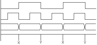 |
| CPU CLOCK | |
| ADDRESS BUS | |
| NGFCDI |
The power supply unit fitted to the BBC Microcomputer is a switch mode type. This unit produces +5 volts at 3.75 amps and -5 volts at 0.1 amps which are supplied to the main printed circuit board (main PCB) via seven flying leads. These leads are connected to the main PCB using 0.11" blade type push-on receptacles. The three red leads carry +5 volts to various points on the board, which are all connected together electrically by copper tracks on the underside. The reason for this is to overcome the need for large, high current carrying, copper tracks on the printed circuit board. The mauve-coloured lead carries the -5 volt supply and the three black leads connect the zero volt line to the board. Note on the early, linear type, supply the -5V lead is coloured brown.
A six pin connector, which is mounted on the case of the power supply unit on the underside of the microcomputer (see photograph chapter 5), provides auxiliary power for accessories such as a floppy disc drive unit. This socket provides a +12 volt supply in addition to the supplies carried to the main PCB. Details of the connections to this socket are given in chapter 5 (fig 5.2).
Early BBC Microcomputers, mainly issues 1 and 2, were fitted with a linear type power supply unit which employed a conventional mains transformer and bridge rectifier, the regulation of the voltage being performed by several 7800 series voltage regulators. These power units tend to get rather hot, even in an unexpanded model A machine and do not provide any auxiliary power. The linear supply can be distinguished from the later switch mode type by its black painted case and the absence of an auxiliary power socket.
Both types of supply contain no user-serviceable components and should therefore be exchanged if they are found to be faulty. The early linear supply should be exchanged for a switch mode type if it overheats or is faulty.
The Microprocessor Unit (MPU) used in the BBC Microcomputer is the 6502A, which is a 2 MHz version of the popular 8 bit 6502, introduced by MOS Technology in 1975. Although a 2 MHz device is used, and indeed many devices such as the Random Access Memory (RAM) are accessed at this speed, the MPU does in fact run at 1 MHz when addressing slow devices within the computer. Examples of these 1 MHz devices are the Versatile Interface Adapters (VIA's) and the Analogue-to-Digital (A to D) converter.
The microcomputer uses a master clock frequency of 16MHz which is generated by a crystal controlled oscillator. The oscillator circuitry is designed around a high speed TTL hex inverter type 74S04 (IC43) . Two of the inverters within IC43 form an RC oscillator which is forced to run at 16 MHz by a 16MHz crystal (X1). The output of this oscillator is buffered by one of the remaining inverters within IC43 before being conditioned by a high speed NAND gate, part of IC40. This provides the 16 MHz clock signal for both the video ULA, the floppy disc circuitry and the serial ULA.
One section of the video ULA is used to subdivide the 16MHz clock into four in-phase signals of 1,2,4 and 8 MHz, thus providing the required clock signals for the remaining circuitry within the microcomputer.
A 6MHz clock is required by the SAA5050 Teletext character generator (IC5) and also the "Econet" circuitry on early versions of the machine. This is produced in a rather unique way using the 4MHz and 8MHz clock signals. A set-reset (SR) bistable is formed using two cross coupled NAND gates (part of IC40) and two inverters (part of ICs 37 and 43) The 8MHz signal is inverted by part of IC37 (74LS04) and fed to one input of the cross-coupled NAND gates. Similarly, the 4MHz signal having been inverted by part of IC43 is coupled via a capacitor/resistor network (C41 and R94) to the other input of the cross coupled NAND gates. This CR network delays the reset action of the bistable thus producing a modified 4MHz waveform (see figure 3.1).
The phase-modified 4MHz waveform produced by the bistable is exclusively ORed (using part of IC38) with the 2MHz clock to produce a 6MHz clock which is "phase-locked" to the master clock. This 6MHz signal contains erroneous pulses which are removed by a CR network coupled to the input of an inverter (IC37, 74LS04)
Figure 3.1 Generation of 6MHz Clock signal:
<p21 left blank for diagram>
The 8-bit 6502A microprocessor can directly address 64 kilobytes of memory. In the BBC Microcomputer, 32 kilobytes of this memory is contained within Read Only Memories (ROM's) . ROM is non volatile; that is, it retains data when the power to it is removed. The Machine Operating System (MOS) of the microcomputer is contained within 15 kilobytes of this read-only memory on a 16 kilobyte device, (normally IC51). The machines address decoding circuitry "maps-out" the remaining 1 kilobyte, since this area is devoted to JIM, FRED and SHEILA. The BASIC interpreter is contained within another mask-programmed, 16 kilobyte ROM (normally IC52).
In early versions of the BBC Microcomputer the 0.1 operating system was contained within four 2732 type 4 kilobyte ultra violet light Erasable Programmable Read Only Memory devices (EPROMs). These were located in IC positions 52,88,100,101, the BASIC interpreter ROM being in IC position 51. In this case the devices were accessed at 1 MHz. The Machine Operating System (MOS) was in EPROM due to delays in producing the mask programmed ROM version. The reason for using four 4K devices was probably due to the high cost of 8K and 16K EPROMs at the time.
Early versions of the series 1 (1.0) operating system, supplied with machines fitted with a disc interface, were contained within two 8-kilobyte EPROMs on a small "carrier board". When replacing this with a Series 1 Operating System ROM it should be noted that the carrier board has rather large diameter pins, which sometimes damage the IC socket into which the board was fitted. Chapter 6 gives details on a remedy for this.
There are positions for five read-only memories on the main PCB, the operating system and BASIC normally occupying two of these, as previously mentioned. The remaining three positions are for fitting utility or additional language ROMs and are often referred to as the "paged" or "sideways" ROM positions. In order to select between these, IC76, which is a 74LS163, must be fitted and two circuit board links removed (see chapter 4). This modification is only required on issues 1,2 and 3 of the main PCB. In order to be able to make use of the paged ROM facility it is also necessary to have a Series 1 Machine Operating System fitted.
If the sideways ROM to be selected is an 8 or 16 kilobyte device, then it can be switched into the ROM memory space by writing to a 74LS163 4-bit synchronous binary counter (IC76), which is referred to as the ROM select latch. In cases where four, 4 kilobyte ROMs are fitted in the paged ROM sockets, a 74LS139 two-to-four line decoder (part of IC20) selects which of the four devices is being selected by lines A12 and A13 of the address bus.
The Model A BBC Microcomputer is fitted with eight 16k by 1-bit random access memory devices in IC positions 53 to 60 providing a total of 16 kilobytes. A further 16 kilobytes of RAM is fitted to the Model B machine in IC positions 61-68 inclusive, thus providing the full 32 kilobytes of RAM.
The RAM devices used are dynamic types. In dynamic RAMS each bit of information is stored as an electrical charge on the gate capacitance of a field effect transistor. The charge on the gate capacitance leaks away with time (typically 2ms) and must therefore be replenished or "refreshed" periodically, in order to retain the data stored in the memory. This is accomplished by activating the Row Address Select (RAS) signal whilst a valid row address is on the address lines. In this way, 256 bytes of RAM are refreshed after each high to low transition of the RAS line.
The 6502A microprocessor, unlike the Z80, does not provide a facility for directly refreshing dynamic RAM and therefore additional circuitry is required. In the BBC Microcomputer the RAS inputs of the dynamic RAMs are continuously activated by the output of a D-type bistable (half of IC44). The 4 and 8MHz clock signals provide the input to this bistable.
The 6845 cathode ray tube controller (CRTC, IC2) or the microprocessor may have control of the RAM address lines. Six octal three-state buffers (IC8 to IC13) are used to select which of these two devices has access to the RAM address lines. The outputs of the dynamic RAMs are enabled when the Column Address Select (CAS) lines are activated.
Control of the RAM address lines is alternately switched between the microprocessor and the CRTC every 250ns. One of the primary functions of the 6845 CRTC is to generate RAM refresh addresses, which it must do in order to refresh the screen. The RAM refresh addresses are generated sequentially and since the CRTC has access to the RAM address lines twice in every microsecond, 512 bytes are refreshed in this period. This method of RAM refreshing is often referred to as "transparent" RAM refresh since it is performed whilst the microprocessor is engaged in internal activity and hence the operation is transparent to it.
The video circuitry of the BBC Microcomputer is designed around three integrated circuits. These are
The 6845 CRTC is used to generate the raster scanned video display and also to refresh the dynamic RAM (see previous section) . The horizontal and vertical synchronisation signals required for the video display are generated by this device. These two signals are fed to the SAA5050 Teletext character generator (IC5) and are also combined by a NOR gate (part of IC41) to provide the composite synchronisation (CSYNC) signal.
In screen modes 1 to 6, the bit patterns for the character fonts are contained within the operating system ROM of the machine. These bit patterns are transferred into screen RAM as required and are latched in to the video ULA at the end of each CRTC access cycle. According to which screen mode is in operation, the video ULA serialises each byte of information read from the screen memory (2 bytes per microsecond) into a 2,4 or 8 bit wide train of pulses. This enables the screen to display modes varying from 640 horizontal pixels in 2 colours (high resolution mode 0) to 160 pixels in 8 colours, which may be flashing (mode 2).
The bit patterns required to produce the graphics images are generated by routines within the operating system and are then stored in the relevant locations in the screen memory. These bit patterns are interpreted by the video ULA in a similar way to the character font information.
Within the video ULA, the serialised bit patterns are presented to a high speed (16MHz) 16 by 4 bit matrix of bipolar memory. This is referred to as the "palette memory". The palette memory is used to relate the logical colour held in the screen memory to the physical colour produced by the RGB output signal.
The technique of storing software generated character and graphics fonts in RAM demands a relatively large amount of user memory (20 kilobytes in the highest resolution modes) . For this reason screen mode 7 is provided which displays high quality text and also limited graphics whilst only using 1 kilobyte of RAM. This is achieved using a Mullard SAA5050 Teletext character generator (IC5) . Each character to be displayed is stored as a single byte in the screen memory as an ASCII code, which is interpreted by the SAA5050. This device then produces the video information, in the form of an RGB signal, to display the corresponding ASCII character on the screen. The RGB signals produced are then fed into the video ULA for the cursor control to be added. Solid state switches within the video ULA are used to route either the Teletext or the internally generated RGB signals to the video driving circuitry.
FIGURE 3.2 RGB SYNTHESIS IN VIDEO ULA
DATA
||
VSERIALISER ||
VPALETTE
64-BIT RAM
(4X16)||
VMULTIPLEXER <= RGB FROM SAA5050 ||
VCURSOR CONTROL ||
V
RGB OUT
A feature of the BBC Microcomputer is its ability to perform a "hardware scroll". The start-address-register within the 6845 CRTC is used to refer to the start address of screen memory. By altering the contents of this register it is possible to scroll the "active" screen display area. In the BBC Microcomputer, the hardware scroll is implemented in a more sophisticated fashion.
Not only is this start address register used, but also an offset can be added to the high order refresh address lines of the CRTC. This offset is specified by the system VIA (IC3), under the control of the operating system, and a two bit code produced via an addressable latch IC32 (74LS259) . This two bit code (C0 and C1) controls a combination of four NAND gates (parts of IC36, 40 and 27) and a full adder IC39 (74LS283) such that the required offset is added to the refresh address lines of the CRTC. The offset to be added is calculated such that by incrementing the CRTC refresh address lines by this amount, the active display area is shifted by one line to reveal the next line where the new data is to be written. Using this technique, the microcomputer can scroll the screen very rapidly.
In screen modes 0, 1 and 2, 20 kilobytes of RAM is required and since sufficient address lines are provided to access 32 kilobytes, this leaves an excess of 12 kilobytes. This poses a problem in that if the start of screen memory were at &3000, (as would be the case in these screen modes) then as the active display area is scrolled upwards, the 20 kilobytes required by the screen would normally enter the area of the memory map which is set aside for ROM. This is prevented by the machine operating system adding 12 kilobytes to the CRTC refresh address lines and thus the active screen display area is wrapped around" within the machine's screen memory. Similarly, in other screen modes the required offsets are added according to table 3.1.
| SCREEN MODE | SIZE | OFFSET |
| 0,1,2 3 4,5 6 |
20K 16K 10K 8K |
12K 16K 22K 24K |
TABLE 3.1
The video uncommitted logic array (IC6) produces red, green and blue signals which after buffering by transistors Q4, 6 and 5, are fed to the 6-pin RGB DIN socket (SK3) via current limiting resistors R112,113 and 111 respectively. A composite of synchronisation signal, which can be selected to be positive or negative going by a circuit board link (S31) , is also fed to this socket along with ground and +5V connections.
The horizontal and vertical components of the composite synchronisation signal are generated by the 6845 cathode ray tube controller chip (IC2). Monitors equipped with red, green and blue (RGB) drive inputs can be connected to this socket. Since the RGB output generated by the computer, is fed to the drivers of the primary colour guns of the picture tube directly, a high quality display is achieved.
In order to drive monochrome monitors equipped with a 1V peak-to-peak composite video input (RS170 standard), the RGB and composite synchronisation signals are summed by resistors R117,R118 and R116 and fed to the base of transistor Q7. The 1 volt peak-to-peak drive required is thus produced at the emitter of this transistor. The phase alternating line (PAL) colour information may be added to the composite video output by the addition of a capacitor or by the bridging of a PCB link (S39), if present (see chapter 4). Connection to the composite video output of the computer is by a standard BNC. type connector (SK2) . It must be stressed that any monitor connected to either the R.G.B. or video BNC sockets must be electrically isolated from the mains supply. The easiest way to check this is to consult the manufactures of the monitor in question.
Colour television receivers usually require a UHF modulated PAL encoded signal. Such a signal is provided by the BBC Microcomputer from the socket marked "UHF out". An Astec UM1233 modulator, which has a video bandwidth of 8 MHz, is used to convert the composite video signal to the required UHF signal.
The PAL encoding is performed using discrete circuitry. A 17.734475 MHz signal is generated by a crystal controlled oscillator consisting of a transistor (Q10) and a 17.734475 MHz crystal (X2). The signal produced, is then inverted using a NAND gate (part of IC50) and divided by four using a 74S74 bistable (IC46) to provide the 4.43361875 MHz colour subcarrier frequency. The quadrature colour-difference signals "U" and "V" are produced on pin 9 of IC46 and pin 11 of IC48 respectively. The horizontal synchronisation pulses produced by the CRTC (IC2) use an exclusive OR gate (part of IC48) to gate the "V" colour difference signal. This produces the required alternating phase signal for each horizontal line scan. Exclusive OR gates (IC47 and IC48) are then used to generate the yellow, cyan, green, magenta, red and blue colours according to the phase relationships of the "U" and "V" signals. These signals are then "mixed" using six NAND gates (IC49 and part of IC50) . The colour burst gate signal is generated using an inverter (part of IC37) and a NOR gate (part of IC4). This arrangement is timed by a CR network (C45 and R189) thus producing a burst gate pulse in the back porch period of the line scan. The burst gate signal is also mixed using the NAND gate mixer.
Errata: the original text quoted the crystal frequency and carrier as 17.73 and 4.4325 MHz respectively. The original author obvious rounded off the former before calculating the latter.
Certain devices within the BBC microcomputer need to be serviced at 1 MHz instead of the normal 2MHz. These devices are:
The circuitry used to perform this function is designed around IC's 23,29,30,3l,33 and 34. Whenever a 1 MHz device requires servicing, the relevant input of an 8 input NAND gate IC23 (74LS30 please note this gate is drawn as a NOR gate with inverted inputs on the Acorn circuit diagram) , is taken low. This results in the output from the NAND gate going to logic '1', which is used to inform the cycle stretch circuitry that a slow access device requires service. The logic '1' is first inverted by part of IC33 (74LS04) before being fed to the set input of a bistable (half of IC31) and also one input of a NOR gate (part of IC29) . This bistable remains set, thus it effectively "remembers" that a slow access has been requested.
The output of the bistable is fed via the NOR gate to the input of another bistable, part of IC34. This second bistable is used to reset the "memory" bistable after a time governed by the phase relationship between the 1 MHz and 2MHz clock signals. Meanwhile, one of the 2 MHz clock cycles will have been masked off by this second bistable. Depending on the phase relationship between the two clocks at the time of the request, the 2MHz clock to the microprocessor will be held at logic '1' for either 3 or 5 half cycles.
The heart of the "Econet" circuitry is IC89, a Motorola MC6854 Advanced Data Link Controller (ADLC).
Connection to the "Econet" network is by a 5-pin l80 degree DIN socket (SK7) on the rear of the machine. The network clock I] connects to pins 3 and 5 of this socket, whilst pins 1 and 4 carry the data. Pin 2 is connected to 0 volts. The data line is bi-directional, thus both transmitted and received data is carried along the same pair of wires in half-duplex mode. Unlike the RS423 serial data transmission port, the "Econet" system uses a differential mode of operation to provide high common mode noise immunity and achieve high transfer rates.
Pin 6 (TXD) of the ADLC feeds the TTL data to be transmitted to one half of a differential line driver (IC93) . provided that this line driver is enabled by the output of IC91, one quarter of which is used as an inverting buffer, data will then be transmitted. The input signal to this inverter comes directly from pin 2 (RTS) of the ADLC.
Any "incoming" data on the data lines is converted to a TTL signal by an analogue comparator (one half of IC94) . The TTL signal is then fed into the received data input (RXD) of the ADLC. In a similar way, the network clock is also detected by the other half of IC94. The output of this comparator feeds both the receive clock and transmit clock inputs of the ADLC. Thus it is not possible to use different receive and transmit baud rates.
The network clock must always be present in order for the ADLC to synchronise correctly, a monostable (half of IC87) is used to achieve this. The time constant of this monostable is such that as long as the clock signal is present it remains permanently triggered. One output of the monostable provides the data carrier detect signal (DCD) into the ADLC, the other output activates the clear to send signal (CTS) via a dual input NAND Schmitt gate. By using this technique, network activity is suspended if the clock signal is interrupted.
Because of the democratic nature of the Econet system it is possible for two or more devices to attempt simultaneously to transmit data on the network. This condition is known as a "collision". A collision on the network will cause the nominal signal level on the data lines to drop because of the increased he loading, this condition is detected by a dual comparator (IC95). The dual comparator arrangement sends a TTL output signal into one quarter of IC91, which is acting as an inverter. The output of this inverter activates the clear to send input of the ADLC via another quarter of IC91, thus transmission is suspended in the event of a collision. Each of the microcomputers involved in the collision will then retry. The condition is detected by both machines and an arbitration algorithm within the "Econet" system software ensures that no two computers will retry simultaneously.
The individual station address is set by the group of links S11, in conjunction with IC96. This is detailed in the chapter 4 which deals with link functions. The "Econet" network must be terminated at each end with its characteristic impedance to prevent signal reflections. On early issue printed circuit boards resistors R26,42,53,54,56, capacitors C19,22 and diode D3 provide this optional termination.
The network clock is usually derived from an external "clock box", however, on some early issue main PCB's, circuitry was provided to enable the network clock to be generated on board. This circuitry consisted of IC90 (4018), IC97 (74LS74) and the normally unused half of IC93. The 6MHz clock signal derived from the output of IC37 is divided by two, using half of IC97 (74LS74). This 3MHz signal is then further subdivided in to a range of frequencies by IC90, link S3 is then used to select the required base clock frequency. Clock base frequencies usually lie in the region 75KHz to 625KHz. The required frequency is dependant on the line length of the network. The base clock frequency is then fed directly in to the input the normally unused half of the line driver IC93. The of this line driver is then connected to the clock output the DIN "Econet" connector and provides the network clock source.
The link S5 is used to enable the clock line driver and link S6 may be used to further subdivide the clock base frequency by 2 or 4.
The keyboard consists of a ten by eight matrix of normally open contact switches which are mounted on a metal plate. Connections to the contacts of these switches are made by a glass-fibre printed circuit board. This board also carries ICs 1, 2, 3 and 4, the loudspeaker, three LED's, the keyboard connector (to PL13) and the ROM cartridge socket (if fitted).
The keyboard circuitry is based on the "walking zero' 0 technique. IC1 is a synchronous binary counter (74LS163) which is clocked by the 1 MHz system clock. The outputs from this IC are decoded by IC3 which is a BCD to decimal decoder (7445). The ten outputs of this decoder are connected to the column lines of the keyboard matrix. In this way, each column in turn is pulsed low then high thus producing the "walking zeros" pattern. Depression of any key results in the output of IC4, an 8 input NAND gate (74LS30), pulsing high as the walking zero passes the column to which that key is connected. The output from IC4 interrupts the microprocessor using the CA2 line of the system VIA (IC3). On recognition of this interrupt, the computer executes the keyboard reading routine to discover which key was depressed. This is achieved by latching the BCD address of each column in turn directly into IC1 using outputs PA0 to PA3 of IC3, the system VIA, thus interrogating each column in turn. At the same time outputs PA4, 5 and 6 of the system VIA are used to load data into IC2, which is a data selector (74LS251) . Each row is selected in turn by the three bit code present on PA4, 5 and 6. The logic level on a particular row appears at the output of the data selector when selected. In this way, the keyboard matrix is scanned for the coincidence created when a key has been depressed.
The cassette interface has two software selectable baud rates, 0 and 1200 baud. The majority of the circuitry for this interface is contained within a custom designed Uncommitted Logic Array (serial ULA-IC7)
The output signal from the cassette recorder enters the microcomputer on pin 3 of the 7-pin DIN socket SKS. Three of the operational amplifiers contained within IC35 (LM324) are used to condition this signal before it is fed into the cassette input (pin 12) of the serial ULA. Once inside the ULA this signal is presented to both a data /clock separator and a run-in header detector.
Solid state switches within the ULA, under the control of the microprocessor, are used to route the logic signal from the run-in detector to the data carrier detect output of the ULA (see fig 3.3). Similarly, the clock and data logic outputs are routed to the receive clock (RXC) and receive data (RXD)
outputs respectively. The RXD, DCD and RXC outputs of the serial ULA are fed into the RXD, DCD and RXC inputs of IC4, an Asynchronous Communication Interface Adapter (ACIA) type MC6850. The ACIA converts the data to a parallel form which is then presented to the data bus of the microprocessor, on demand.
The cassette clock signals are derived from the 16MHz master clock. The 16MHz signal is firstly divided by 13 using a 74LS163 synchronous binary counter (IC42) and then further subdivided within the serial ULA.
The data to be saved on to the cassette recorder is taken from the data bus and converted into serial form by the ACIA. This serial information is then fed into the TXD input of the ULA. Within the ULA, the serial data is converted to a synthesised sine wave signal, suitable for feeding to a standard cassette recorder. The synthesised sine wave signal is buffered using an operational amplifier (part of IC35) and then fed to pins 1 and 4 of the DIN cassette connector via a DC blocking capacitor (C34)
The CASMO (cassette motor) output of the serial ULA drives a transistor (Q3) which in turn operates the cassette motor relay and also the keyboard "cassette" lamp (LED). The normally open contacts of this relay are used for automatic motor control switching of the cassette recorder. The connections from these contacts are available on pins 1 and 7 of the cassette DIN socket (SK5).
The solid state switches within the serial ULA are used to route either the cassette signals or the RS423 signals to the ACIA. This switching is determined by the control register of the ULA which is controlled from the data bus. The serial ULA also contains the programmable baud rate generator which is required by the RS423 interface.
The Data Out (D OUT) and Request to Send (RTS) signals from the ULA are converted from a TTL level to RS423 compatible form by a DS3691N line driver (IC75). This device requires both a +5 and -5 volt supply. The data-in (DIN) and clear-to-send (CTS) input signals from the RS423 interface are converted from RS423 to TTL levels by a line receiver IC type DS88LS120N (IC74).
Connection to the RS423 interface is by a 5-pin DIN "domino" socket (SK4)
FIGURE 3.3 SERIAL UNCOMMITTED LOGIC ARRAY
The BBC Microcomputer was designed for use with either one or two 5 1/4 inch or 8 inch floppy disc drive units. These drives may be single or double sided.
In order to use floppy disc drives with the BBC Microcomputer, the disc interface circuitry must be fitted to the main PCB of the machine (see chapter 6). The heart of the floppy disc interface is an Intel P8271 Floppy Disc Controller (FDC) chip (IC78). This device controls data exchange between the floppy disc drive unit and the data bus of the microcomputer. An interrupt generated by the FDC acts on the non-maskable interrupt (NMI) line of the microprocessor (IC1) . Note that apart from the FDC, there are two other devices within the microcomputer which generate NMI signals. These are the "Econet" interface and some 1 MHz bus peripherals.
The TTL output signals from the FDC are fed into open collector NAND buffers, type 7438 (IC79 and IC80) . The outputs from these buffers connect to the disc drive unit via the disc interface plug (PL8) . The data input (Read Data) and index pulse (Index) signals from the floppy disc drive enter the microcomputer on pin 30 and pin 4 (5 ¼ inch drive) respectively. In the case of an 8 inch drive, the index pulses enter on pin 8 of this connector. The option of whether the index pulse input to the P8271 FDC is taken from pin 4 (5 ¼ inch drive) or pin 8 (8 inch drive) of the connector is selected by a PCB link (S10)
The unseparated data signal from the floppy disc drive is fed into one half of a 74LS123 monostable (IC87) , which "stretches" the incoming pulses to a length determined by the time constant of R33 and C13. The outputs of this monostable then feed into a data separation circuit consisting of a dual four-bit binary counter (IC81) and a triple 3-input NAND gate (IC82) . This arrangement produces the "data window" signal which is fed to pin 26 of the FDC. The negated output of IC87 also supplies the read data input to the FDC.
Link S27 is used to route either the 8MHz (5 ¼ inch drive) or the 16MHz clock signal (8 inch drive) from the video ULA into one input of a 74LS393 dual 4-bit binary counter (IC86) . The divide by four (QB) output of this counter provides the clock input to the FDC. Thus either a 2MHz or 4MHz FDC clock is provided, depending on which drive size is to be used. The remaining half of IC86 further sub-divides the FDC clock to produce either a 31.25KHz or 62.5KHz signal. This signal is then used in conjunction with IC83, IC84 and IC85 to detect the drive index pulses and to determine when the drive is ready for a read or write operation.
IC69 is a 6522 Versatile Interface Adapter (VIA) which is used to provide both a standard Centronics parallel printer interface and the user port on the BBC Microcomputer. The printer port uses lines PA0 to PA7 of this VIA, which are buffered by an octal 3-state driver (IC70) . Thus, because this driver is fitted, the printer port may only be configured as an output device. When this port is not being used to drive a printer, it may well be used for driving other user output devices (e.g. a digital-to-analogue converter)
The remaining eight lines (PB0 to PB7) of the user VIA allow the user to interface devices which produce digital signals to the computer. This port can be configured to be an output port or an input port, the option being software selectable.
For further details on the 6522 VIA consult the comprehensive data sheet given at the end of this book.
When the BBC Microcomputer is switched on, a capacitor (C10) is charged up by a resistor (R20) which is connected to the +5V power supply rail. The signal at the junction of the CR network provides a reset signal (RSTA) , which is low at switch-on and rises to +5V when the capacitor is fully charged. Whenever the break key is pressed and also on power up, a timer integrated circuit, type LM555 (IC16) , produces another reset signal (RST).
The RSTA reset signal is only used to reset the system VIA (IC3) whilst the RST signal is a general reset signal which is used throughout the remaining circuitry. In this way the operating system can interrogate the system VIA to determine whether the reset signal was produced at power-up (RSTA) or simply by the break key (RST)
A four channel, dual-slope integrating, 12-bit Analogue-to-Digital Converter (ADC) , type PD7002 (IC73) , is used to convert analogue signals to the digital form required by computer's data bus. The digital outputs of this device are connected directly to the system data bus. The end-of-conversion (EOC) signal from the ADC is fed to the CB1 input (pin 18) of the system VIA (IC3) , which then requests an interrupt (IRQ) .
The ADC derives its reference voltage (Vref) from the forward voltage drop across three silicon diodes connected in series (D6, D7 and D8) . A resistor (R71) limits the current through these diodes.
Connection to the inputs of the ADC is by a printed circuit board mounted, fifteen way, "D-type" connector socket (SK6). This socket also carries the connections to the light pen strobe input of the 6845 cathode ray tube controller (IC2) and the joystick "fire" buttons.
The voice synthesiser used in the BBC Microcomputer is a Texas Instrument two chip set, comprising of a microprocessor-bus compatible Voice Synthesis Processor (VSP) type TMS5220 (IC99) and a Voice Synthesis read-only Memory (VSM) containing speech data, type TMS6100 (IC98) . Speech data for the VSP can be taken either from the VSM or from a slow (1 MHz) data bus which is provided by port A of the system VIA (IC3) . Interrupt (INT) and ready (RDY) output signals from the VSP are fed to lines PB6 and PB7 of the system VIA, respectively. Thus the VSP is under software control.
The speech data inside the VSM is a digitised form of the originally recorded human speech. In order to keep memory requirements to a minimum, this data is a compressed form of the original digitised speech data. The compression technique used is pitch excited Linear Predictive Coding (LPC). The data from the VSM is decoded within the VSP to reconstruct the digital speech information. An 8-bit digital-to-analogue converter inside the VSP provides the analogue speech signal, which is then filtered using an operational amplifier based filter (part of IC17) . The filtered signal is then mixed with the analogue signals from the 1 MHz bus and sound generator before amplification by the LM386 power amplifier (IC19) details of which are given in the following section.
The four-channel sound effects facility on the BBC Microcomputer is provided by a microprocessor-bus compatible sound generator integrated circuit type SN76489AN (IC18) . This device is accessed at 1 MHz by the system VIA (IC3) . The pitch and attenuation of each channel is therefore under the control of the microprocessor. The 4MHz clock from the video ULA provides the clock input to the sound generator.
The audio output signal from the sound generator is mixed with the other audio signals generated by the microcomputer, thus providing a composite sound signal. This signal is then amplified and filtered using analogue circuitry based on operational amplifiers within an LM324 integrated circuit (IC19). The resulting analogue signal is fed to PL16, which is the low-level (DIN) audio output connector. The same signal is also fed to a pre-set potentiometer (VR1) , which acts as a volume control for the internal power amplifier of the computer. This power amplifier is a low supply voltage device, type LM386 (IC19).
In addition to the high speed "Tube" interface the BBC Microcomputer also has a 1 MHz extension bus. Connection to this interface is through PL11 on the underside of the machine. The 1 MHz extension bus provides buffered address lines A0 to A7 (IC71), buffered bi-directional data bus lines D0 to D7 (IC72) and numerous control lines. The interface also has an analogue input line which is fed to the machines internal audio amplifier (IC's 17 and 19) and loudspeaker. The input impedance of this analogue input is 9 kilohms. If the speech and internal sound generator systems are not in use then a signal of + 3 volts RMS will produce full volume output at the loudspeaker. This input level will need to be reduced in order to avoid excessive distortion if the speech and sound generator systems are in use at the same time. There are two other lines on the 1 MHz bus connector which will require further explanation, these are the lines NPGFC (Not PaGe &FC) and NPGFD (Not PaGe &FD) which are often referred to as FRED and JIM respectively.
This signal is decoded from the machines address bus such that when the address bus holds a valid address in the range &FC00 to &FCFF this line will go low. The microcomputer address decoding circuitry around IC20 (74LS139) is used to accomplish this. FRED is intended for use by peripheral devices with small memory requirements.
There are various links within the machine that can be used to enable/disable FRED (S17) or alter its access times (S16) Further information on these links is given in chapter 4.
Acorn Computers Ltd. have standardised on particular addresses in the range &FC00 to &FCFF (FRED) to be used for specific functions, at the present time these are as follows:
TABLE 3.2
&FC00 - &FC0F Test hardware use.
&FC18 - &FC13 Teletext use.
&FC14 - &FC1F Prestel use.
&FC20 - &FC27 IEEE 488 interface (Control Universal Ltd.).
&FC28 - &FC2F Future Acorn expansion.
&FC30 - &FC3F Cambridge Ring interface.
&FC40 - &FC47 Winchester disc interface.
&FC48 - &FC7F Future Acorn expansion.
&FC80 - &FC8F Test hardware devices.
&FC90 - &FCBF Future Acorn expansion.
&FCC8 - &FCFE User applications.
&FCFF         JIM paging register (see JIM)
Normally devices attached to the 1 MHz bus should decode the address lines A0 to A7 and also the NPGFC line (FRED) . In most cases the signal on the NPGFC line will need to be "cleaned up" by one of the circuits shown in figure 3.5 below.
The reason that the NPGFC and NPGFD signals need to be cleaned up is because of the difference in the speed that the 1 MHz bus is running at, compared to the speed at which the machines internal 6502A processor is running. The machines internal processor runs at a clock speed of 2 MHz unless a slow speed device, such as the 1 MHz bus, is being accessed. Circuitry within the BBC Microcomputer is used to effectively "stretch" the 2 MHz normal 6502A clock cycle into the 1 MHz clock (1 MHz E) cycle, required by 1 MHz peripheral devices attached to the 1 MHz bus. This circuitry is described in some detail above.
The NPGFC signal (FRED) produced by the microcomputer's internal circuitry suffers from two distinct problems, these are "glitches" and "double accessing. Refer to diagram 3.4 below.
Figure 3.4 Timing Diagram (1 MHz)
1 MHz CPU CLOCK ADDRESS BUS NGFCDI
The machines internal address bus will normally only change state when the 2MHz clock (2MHz E) is low. It can be seen from figure 3.4, however, that when the address bus changes state the 1 MHz E clock is alternately high then low. This results in low-going "glitches" being produced in the NPGFC signal. These glitches are marked X and Y in figure 3.4. The glitches which occur when the 1 MHz E clock is low (marked Y in figure 3.4) are normally of no consequence but the glitches occurring when 1 MHz E is high (marked X in the diagram) may cause the chip select inputs of the various IC's on the 1 MHz peripheral device to be spuriously activated. One of the circuits shown in figure 3.5, below, can be used to eliminate this problem.
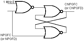
FIGURE 3.5A CLEANING UP PAGE SELECT LINES
1 MHz E NPG- CNPG- 0 0 0 0 1 1 1 falling 1 Unchanged rising 0 0 1 1 1
The circuit shown in figure 3.5 (a) is basically a gated S-R flip flop which will only allow the clean NPCFC/D signal to be low when 1 MHz E is low. This same circuit can be used to clean up the NPGFD (JIM) signal which is also subject to a similar "glitch" problem.
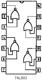
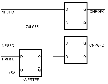
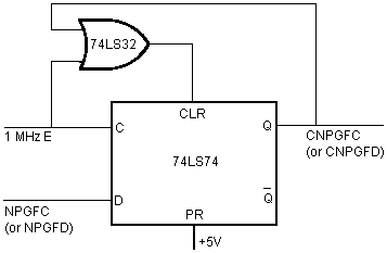
There are also other circuits shown below in figure 3.5 (b) and (c). Figure 3.5 (b) uses a single integrated circuit and allows both FRED and JIM to be cleaned up. Figure 3.5 (c) is an alternative to 3.5 (a).
FIGURE 3.5B CLEANING UP PAGE SELECT LINES
FIGURE 3.5C CLEANING UP PAGE SELECT LINES
It is possible for a peripheral device, which is attached to the 1 MHz bus, to be accessed twice by the CPU. This happens as a result of the way in which the pulse stretching circuitry within the microcomputer works. Basically, it occurs because the CPU clock is in fact held high until the falling edges of the 1 MHz clock and the 2 MHz clock are coincident. If a 1 MHz peripheral is accessed when the 1 MHz clock is high then this peripheral will be given almost immediate access to the CPU. However, because of the fact that the CPU clock is held high, waiting for the coincident edge, the peripheral device will be accessed for a second time when the 1 MHz clock next goes high. This characteristic will not normally be a problem unless the peripheral is reading or writing to a device in order to change the state of an interrupt flag, for instance. This could result in an interrupt going unrecognised.
The NPGFD signal is very similar to the NPGFC line the only difference being that this line is active when the address bus holds a valid address in the range &FD00 to &FDFF. As with FRED this signal also suffers from glitches and must, therefore, be cleaned up using a similar clean up circuit to one of those shown in figure 3.5.
The NPGFD line is intended to be used in conjunction with the paging register in FRED (address &FCFF) to allow the machine to address up to 64k of additional memory. This memory would normally be accessed one page (256 bytes) at a time, the paging register in FRED (at address &FCFF) would contain the page number i.e. up to 256 pages each with 256 bytes. The value contained in the paging register is referred to as the "Extended Page Number" (EPN)
Acorn Computers Ltd. have adopted a convention for use of the extended pages which presently is as follows
EPN's. Allocation. 0 to &7F
&80 to &FFReserved for use by Acorn.
General user applications.TABLE 3.3
On power up or hard break the contents of the paging register are set to 0.
Acorn Computers Ltd. have issued certain guidelines which should be adhered to when designing devices to attach to the 1 MHz bus, these are summarised as follows;